 |
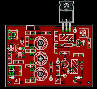
| This is the hole pattern for copper clad board proto |
This is an archived blog I have of my 20 Meter - 6 Meter HF / SSB QRP radio project (Model 620) Check back later as I am in the process of recovering this blog from a defunct AT&T site! I have most of the pictures I loaded to the old FTP site...and the text is on its way a bit at a time
Tuesday, April 29, 2008
Saturday, April 19, 2008
M620 - Power Amp
PART 4 – RF/PA Board Construction
The concept is to provide enough power, hopefully a couple of Watts, to allow the transceiver to be heard someday on the bands! The RF board is designed only to provide a few (hundred?) milliwatts of output. The design trick here is to provide a reasonable amount of power without quickly draining all the battery power. A 5W transmitter can easily draw several Amps of power. The PA board also has a LPF, to keep us legal as far as spurious emissions, and provide T/R switching. The “extra” cap across the output inductor and careful tuning really helps the efficiency, as this filter matches the output of the amplifier to the antenna as well as suppressing the harmonics. This board is a simple linear FET amp basically copied from one of the many in the literature, but in a form factor we can fit. This is one circuit that probably demands more attention, but works fine for now.
Build test the circuits by injecting a small RF signal and tuning the LPF and amp bias set just to have enough power out to see the RF output using a scope or the power detection circuit connected to a DVM. Moving the LPF coil’s windings closer together one at a time tunes the filter. This takes a little time, but this circuit can deliver over 5W when carefully adjusted. Conversely, if the inductors are off by even one turn the efficiency will be very poor. For the final tuning I connect the LPA to the RF board and the output to a dummy load. To inject the test signal I use a stereo phone connector with a mono jack to disable the internal microphone on the RF board’s test connector (JP11) the tip is the CW signal and the ring disables the microphone output, at it ground to the sleeve when a mono jack is used. Only key the PTT switch for quick measurements being careful not to overheat the LPA’s transistors. The CW level is adjusted from zero and increased until the power stops rising, then back off the injected signal until the output falls. Then final adjustments can be done for max power. I actually use a PC soundcard with a CW program for this signal.
M620 - DDS/Controller Board
PART 2 – VFO Controller Board Construction
The concept of the controller board is to provide a simple and stable local oscillator source controller as well as providing a user interface and some metering capability. Typically these bands use a frequency doubled VFO, which are usually touchy, or Crystal
The other main components that the proto design uses are a SMT PIC 16F88 [A] and the AD9851 DDS [B] plus a rather curious combination of other thru-hole and SMT parts. The main reasoning for some parts which could only be found in SMT and some are simply what I had on had to build up several boards.
Building the board using a technique using fine wire solder on each IC pin, followed by a solder wick to clean up any shorts between the pins worked quite well for soldering the ICs. Once the board is built, it is programmed via the provided programming header [G]. Install the LCD directly to the controller board after some perliminary testing.Friday, April 11, 2008
Subscribe to:
Posts (Atom)


